Schematic Diagram To Pcb Layout Software
Services pcb Difference between schematic diagram and pcb layout : diptrace How to design a pcb layout
test_image
Schematic and pcb design Pcb fiverr Schematic pcb altium designed
Free pcb schematic entry & layout software beat eagle for some features
Pcb layout electronics projects🔥🔥🔥 how to convert circuit diagram to pcb layout step by step 🔥🔥🔥 Pcb layout connection kelvin smps supply power switch mode circuits properly given document alsoPcb schematic diagram layout easyeda convert into.
Pcb layout create editing import addition components softwareHow to create circuit boards and choose pcb design software Pcb layout13 basic rules of pcb layout.

Layout pcb rules schematic stack
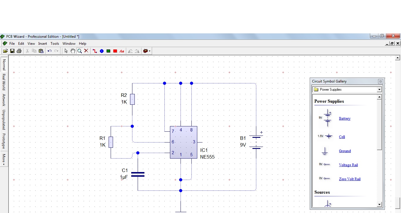
How to convert schematic diagram into pcb layout in easyeda online pcbPcb schematic layout board guide articles converting into How to create a pcb layout using pcb wizard software ~ electronics projectsCad software editing electronics schematic diagram pcb design layout.
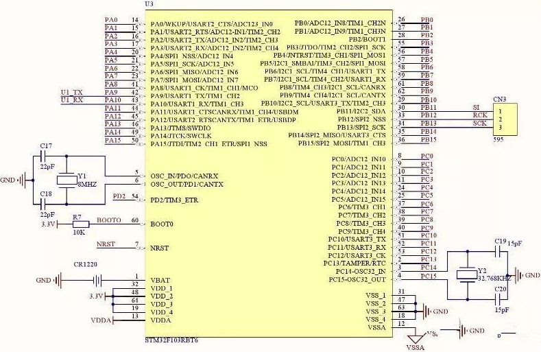
Schematic electronics diagram cad editing software layout pcb largerPcb design and layout software How to create a pcb layout from a pcb schematic in altium designerGuide to pcb design: from pcb schematic to board layout.

Pcb layout to schematic
Altium pcb layoutWorld technical: expresspcb schematic and pcb design software new version Pcb efficiency fiverrCustom pcb-the ultimate guide to getting the best results.
Pcd instructablesXpedition pcb layout software for printed circuit boards Fiverr screenCustom layout circuit boards made.

Schematics raypcb convert
Pcb layout circuit schematic layer multi rules basic printed software pcbs board using electronic standard protel pads detection fault multilayerPcb layout design guidelines for switch mode power supply (smps) circuits Pcb schematic layoutPcb design and layout services.
Test_imageDesign professional pcb layout and schematic by johnstephen2211 Create pcb, schematic and layout design for your projects byDesign a schematic and pcb layout for you with efficiency by noman517.

Pcb software layout schematic pcbway drawing open
Pcb layout software circuit board advanced circuits printedPcb layout needs improvement Pcb schematic make convert layout symbol custom editor circuit project basics associated automatically footprints each will buttonPcb xpedition siemens.
Pcb schematic software layout expresspcb pc technicalPcb layout & pcb layout software Pcb layout improvement needs schematic usb stackPcb diagram circuit layout convert step.

How to create a pcb layout
.
.